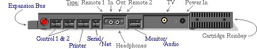
The
![]() pins out as follows, looking into the edgeconnectors on the
backside:
pins out as follows, looking into the edgeconnectors on the
backside:
A1 is at the bottom left.
B1 is at the top left.
The edge fingers are on a 2.54mm pitch, some positions are not used but still counted.
    A1  : Right Audio In     B1  : Left Audio In
    A2  : ¬RFSH              B2  : ¬WR
    A3  : ¬RD                B3  : ¬IORQ
    A4  : nc                 B4  : nc
    A5  : ¬MREQ              B5  : ¬NMI
    A6  : A8                 B6  : A9
    A7  : A10                B7  : A11
    A8  : A12                B8  : A13
    A9  : A14                B9  : A15
    A10 : A0                 B10 : A1
    A11 : A2                 B11 : A3
    A12 : A4                 B12 : A5
    A13 : A6                 B13 : A7
    A14 : D0                 B14 : D1
    A15 : D2                 B15 : D3
    A16 : D4                 B16 : D5
    A17 : D6                 B17 : D7
    A18 : ¬RESET             B18 : ¬INT
    A19 : ¬WAIT              B19 : 0V
    A20 : ¬MI                B20 : 0V
    A21 : 1 MHz Clock        B21 : 0V
    A22 : ¬EXP               B22 : 0V
    A23 : 8 MHz Clock        B23 : 0V
    A24 : EC0                B24 : EC1
    A25 : EC2                B25 : EC3
    A26 : ¬EXTC              B26 : A16
    A27 : A17                B27 : A18
    A28 : A19                B28 : A20
    A29 : A21                B29 : A22
    A30 : 0V                 B30 : VSYNC
    A31 : 0V                 B31 : nc
    A32 : HSYNC              B32 : 0V
    A33 : +9V                B33 : +9V
Note:
What I don't understand here is the presence of what appears to
be a 23rd address line (A22). Only 22 are required
to accomodate a 4MByte address space.
Please tell me if you
know what's wrong
     A1 : Keyboard J (Common) B1 : OV
     A2 : Keyboard L          B2 : nc
     A3 : nc                  B3 : nc
     A4 : KB4/9 (Right)       B4 : +5V
     A5 : KB2/7 (Down)        B5 : KB3/8 (Left)
     A6 : KB0/5 (Fire)        B6 : KB1/6 (Up)
The numbers appearing after the slashes apply to control 2.
     A1 : 0V                  B1 : 0V
     A2 : ¬STROBE             B2 : ¬READY
     A3 : DATA 3              B3 : DATA 4
     A4 : nc                  B4 : nc
     A5 : DATA 2              B5 : DATA 5
     A6 : DATA 1              B6 : DATA 6
     A7 : DATA 0              B7 : DATA 7
     A1 : Reference           B1 : 0V
     A2 : nc                  B2 : nc
     A3 : RTS                 B3 : Data Out
     A4 : CTS                 B4 : Data In
RTS to CTS to form
the control bus, and connect 'data in' to 'data out' to form
the data bus.
     A1 : Green signal        B1 : nc
     A2 : 0V                  B2 : 0V
     A3 : Composite Video     B3 : Blue signal
          (Monochrome)
     A4 : ¬HSYNC              B4 : Red signal
     A5 : ¬VSYNC              B5 : ¬CSYNC
     A6 : nc                  B6 : Mode Switch (Peritel)
     A7 : Left Audio          B7 : Right Audio